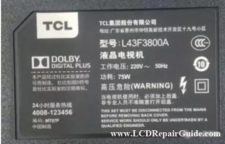
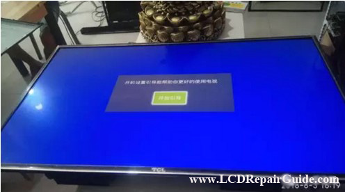
A TCL L43F3800A-MT07P Smart LED TV with Problem Cannot Boot/Start-up
Author: iFix A little busy recently, but someone send a Smart TV to me for repair, the TV model is TCL L43F3800A--MT07P.
Symptom: The indicator LED light up, but it can’t boot/start-up. The voltage output from power supply PSU is normal, so give the judgement that the fault location is on the main board.
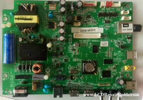
For this TV main board, at the beginning, I can’t fix it yet. But recently I have learned more and repaired a lot, so I am already familiar with it. Remove the cover, and measure the power supply of all DC and LDO, all are normal. This TV, the memory model is Toshiba 5D1K, EMMC bad is a common problem, so I began to confidently deal with EMMC. There was a backup before, just take a piece of EMMC and write it offline through RT809H programmer.
Power on the TV mainboard, and have a test, but still same problem! After power on, although the LED indicator light on, there’s no flicker, which means that, the board is not working properly. Is there a problem with the chip or the welding? Do again, I take a chip to rewrite, and then install back, but the problem remains the same. What’s a pity, the judgment is wrong? It seems that I can’t rely on experience to repair the mainboard!
Let’s see the Print-Log (print information) of the mainboard, its TX, RX is at the USB interface. I forgot to take the picture, weld the transfer line, and connect to RT809F. Select the Serial Print to get their Print-Log information to find what the problem is occur in the TV mainboard. Below is the result read from their Print-Log:
=============================================== 2018-8-3, 15:12:23 COM9, BaudRate:115200 bps, RXD: VGA->15,TXD: VGA->12, Printed byRT809F:
Boot- DRAM Channel A Calibration. 1T = (79 - 17) = 62 delay cells Clock frequency = 798 MHz, Clock period = 1253 ps, 1 delay cell =20 ps Byte 0 : Gating(-31 ~ 32), Size=64 . Byte 1 : Gating(-31 ~ 31), Size=63 . Byte 2 : Gating(-31 ~ 32), Size=64 . Byte 3 : Gating(-31 ~ 32), Size=64 . error on bit 0 ,setup_time =hold_time =0!! error on bit 1 ,setup_time=hold_time =0!! error on bit 2 ,setup_time=hold_time =0!! error on bit 3 ,setup_time=hold_time =0!! error on bit 4 ,setup_time=hold_time =0!! error on bit 5 ,setup_time=hold_time =0!! error on bit 6 ,setup_time=hold_time =0!! error on bit 7 ,setup_time =hold_time=0!! error on bit 8 ,setup_time=hold_time =0!! error on bit 9 ,setup_time=hold_time =0!! error on bit 10 ,setup_time=hold_time =0!! error on bit 11 ,setup_time=hold_time =0!! error on bit 12 ,setup_time=hold_time =0!! error on bit 13 ,setup_time=hold_time =0!! error on bit 14 ,setup_time=hold_time =0!! error on bit 15 ,setup_time=hold_time =0!! error on bit 16 ,setup_time=hold_time =0!! error on bit 17 ,setup_time=hold_time =0!! error on bit 18 ,setup_time=hold_time =0!! error on bit 19 ,setup_time=hold_time =0!! error on bit 20 ,setup_time=hold_time =0!! error on bit 21 ,setup_time=hold_time =0!! error on bit 22 ,setup_time=hold_time =0!! error on bit 23 ,setup_time=hold_time =0!! error on bit 24 ,setup_time=hold_time =0!! error on bit 25 ,setup_time=hold_time =0!! error on bit 26 ,setup_time=hold_time =0!! error on bit 27 ,setup_time=hold_time =0!! error on bit 28 ,setup_time=hold_time =0!! error on bit 29 ,setup_time=hold_time =0!! error on bit 30 ,setup_time=hold_time =0!! error on bit 31 ,setup_time=hold_time =0!! HW Byte 0 : DQS(0 ~ 0), Size 0 ,Set 0. HW Byte 1 : DQS(0 ~ 0), Size 0 , Set 0. HW Byte 2 : DQS(0 ~ 0), Size 0 , Set 0. HW Byte 3 : DQS(0 ~ 0), Size 0 , Set 0. RX DQ/DQS calibration fail! DATLAT calibration no DATLAT taps pass default tx dq PI delay value(16) is fail on bit 0!! default tx dq PI delay value(16) is fail on bit 1!! default tx dq PI delay value(16) is fail on bit 2!! default tx dq PI delay value(16) is fail on bit 3!! default tx dq PI delay value(16) is fail on bit 4!! default tx dq PI delay value(16) is fail on bit 5!! default tx dq PI delay value(16) is fail on bit 6!! default tx dq PI delay value(16) is fail on bit 7!! default tx dq PI delay value(16) is fail on bit 8!! default tx dq PI delay value(16) is fail on bit 9!! default tx dq PI delay value(16) is fail on bit 10!! default tx dq PI delay value(16) is fail on bit 11!! default tx dq PI delay value(16) is fail on bit 12!! default tx dq PI delay value(16) is fail on bit 13!! default tx dq PI delay value(16) is fail on bit 14!! default tx dq PI delay value(16) is fail on bit 15!! default tx dq PI delay value(16) is fail on bit 16!! default tx dq PI delay value(16) is fail on bit 17!! default tx dq PI delay value(16) is fail on bit 18!! default tx dq PI delay value(16) is fail on bit 19!! default tx dq PI delay value(16) is fail on bit 20!! default tx dq PI delay value(16) is fail on bit 21!! default tx dq PI delay value(16) is fail on bit 22!! default tx dq PI delay value(16) is fail on bit 23!! default tx dq PI delay value(16) is fail on bit 24!! default tx dq PI delay value(16) is fail on bit 25!! default tx dq PI delay value(16) is fail on bit 26!! default tx dq PI delay value(16) is fail on bit 27!! default tx dq PI delay value(16) is fail on bit 28!! default tx dq PI delay value(16) is fail on bit 29!! default tx dq PI delay value(16) is fail on bit 30!! default tx dq PI delay value(16) is fail on bit 31!! error: cannot find right boundary of DQM error: cannot find left boundary of DQM TX HW Byte 0 : DQS(-16 ~ -16), Size 1, Set 48. TX HW Byte 1 : DQS(-16 ~ -16), Size 1, Set 48. TX HW Byte 2 : DQS(-16 ~ -16), Size 1, Set 48. TX HW Byte 3 : DQS(-16 ~ -16), Size 1, Set 48. TX DQ/DQS calibration fail!
=============================================== Is there a problem with the main chip MSTAR control? This print-log information doesn’t seem to be the same as any other board before, I was confused, so I decided to change the main chip, to see if it is work or not.
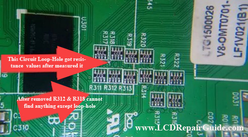
Unfortunately, the result is still same problem, it cannot work. If the problem just like what I do just now, it is so easy that there is no need to post. That’s my last method, consult with master Luo. Master Luo clearly pointed out it is the DDR communication failure! (For the Print-Log info, you can refer to the V5.0-OLED/LED/LCD TV Repair Tips ebook). So I start to measure right now, measure their network resistance value to ground. Normally, the network resistor all values must same. Then I found that one row is not normal. Every resistor is 380 or 0.380 (use multimeter DIODE range to measure), only one resistor is 670!
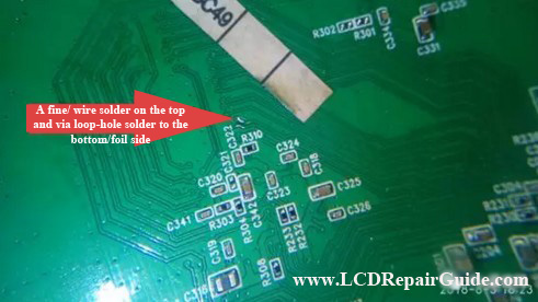
Disconnect the resistance and find out the abnormal point. After removing the resistance with the hot are gun, it was found that the resistor value of the abnormal one was 410 now, which was close to normal. It shows that the possibility of circuit loop-hole is very high. There is a significant resistance from the front to the bottom side of the mainboard circuit loop-hole. It seems that the problem has been found. Use the drill machine with the 0.25MM bit, the hole was perforated, and the bit was successfully left in the circuit loop-hole.
Pull out the sacrificial bit and find a fine copper wire to solder from top to the bottom/foil side as photo below:
Everything checks okay, after that power on the TV, the LED indicator light turns dark. Press the remote control power button, TV can start-up now with the light LED indicator. The programmers can show the print-log now and obviously getting normal. The Print-Log like below:
============================================== 2018-8-3, 15:57:34 COM9, BaudRate:115200 bps, RXD: VGA->15,TXD: VGA->12, Printed by RT809F:
Boot- DRAM Channel A Calibration. 1T = (81 - 17) = 64 delay cells Clock frequency = 798 MHz, Clock period = 1253 ps, 1 delay cell =19 ps Byte 0 : Gating(-32 ~ 33), Size=66 . Byte 1 : Gating(-32 ~ 32), Size=65 . Byte 2 : Gating(-32 ~ 33), Size=66 . Byte 3 : Gating(-32 ~ 33), Size=66 . HW Byte 0 : DQS(-11 ~ 13), Size 25 , Set 1. HW Byte 1 : DQS(-13 ~ 12), Size 26 , Set 0. HW Byte 2 : DQS(-9 ~ 14), Size 24 , Set 3. HW Byte 3 : DQS(-11 ~ 14), Size 26 , Set 2. DATLAT calibration first_step= 11 total pass= 5 best_step=12 . TX HW Byte 0 : DQS(3 ~ 26), Size 24, Set 14. TX HW Byte 1 : DQS(3 ~ 27), Size 25, Set 15. TX HW Byte 2 : DQS(2 ~ 24), Size 23, Set 13. TX HW Byte 3 : DQS(1 ~ 26), Size 26, Set 13. DRAM A Size = 768 Mbytes. Boot
Start Pmain
0x0000a000 EMMC boot
CID:0xc6cd5287 :0x30006a8d :0x30344745 :0x11010030 LZHS addr:0x00100040 LZHS size:0x0015e408 LZHS checksum:0x000000e7 LZHS size:0x0015e408 store RSA & AES keys in DMX SRAM LZHS begin Boot
Start Lmain
MT5882 Boot Loader v0.9
===============================================
Since the print-log is so long, so that I omit it here. Installation back the mainboard to TV and it is show the image perfectly. Finally, connecting network to upgrade the latest version firmware of Mainboard, and it was repaired perfectly as photo below:
Conclusion: If you didn’t have the knowledge on how the Tv works and how to troubleshoot/isolate TV problem, it will waste you lots of time and money spend on the chips and etc. So this TV mainboard case even is just their circuit loop-hole problem (spare part cost is just a wire only), but if you don’t know how to check or troubleshoot it, finally, I believe you will just replace a whole TV mainboard with expensive repair cost! For more details on the Print-Log information, please refer to V5.0-OLED/LED/LCD TV Repair Tips ebook.
Best Ebooks to learn Troubleshooting & Repairing LED/LCD TV Mainboard
2018 LCD/LED Screen Panel Repair Guide
Learn the Basic info for LCD & LED TV T-con Repair and TV Mainboard repairing information. It will helps to you in LCD & LED TV Repair!
PV1-Plasma TV Repair Tips Ebook by Kent Liew:
|
|
